
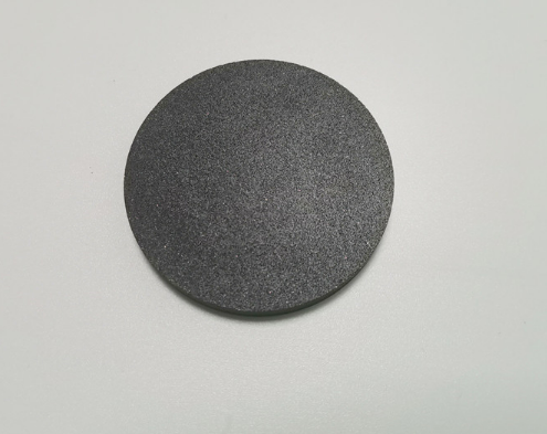
Silicon Carbide Sputtering Target
Silicon Carbide Sputtering Target is made from silicon carbide (SiC) with high purity and a uniform microstructure, widely used in semiconductor, optoelectronics, thin-film deposition, and other high-tech fields. As a leading supplier andmanufacturer of premium silicon carbide products, we can supply high-quality silicon carbide sputtering targets with various specifications and competitive prices, offering customized solutions to meet specific requirements.
- Custom and standard options available.
- Fast lead times guaranteed.
- High performance at a competitive price.
Silicon Carbide Sputtering Target Data Sheet
| Purity: | 2N5-4N |
| Color: | Black or Dark grey |
| Chemical Formula: | SiC |
| Material Grades: | Reaction Bonded SiC, Pressureless Sintered SiC, Hot-pressed SiC, etc. |
| Density: | >3.2 g/cm³ |
| Dimension: | Diameter (inch) : 1, 2, 3, 4, 5, or customized Thickness (mm): 1, 2, 3, 4, or customized |
| Shape: | Rectangular, Disc, or Tube |
| Bonding Service: | Unbonding or Bonding |
Silicon Carbide Sputtering Target Description
Silicon Carbide (SiC) primarily exists in two crystal structures: the cubic β-SiC and the hexagonal α-SiC. Compared to other ceramics such as alumina (Al2O3) and boron carbide (B4C), SiC exhibits superior mechanical properties, better oxidation resistance, higher wear resistance, and a lower friction coefficient. Silicon Carbide Sputtering Target is made from high-purity silicon carbide (up to 99.99%). Its high purity and uniform microstructure allow it to maintain stable performance in high-energy environments, ensuring an efficient and precise deposition process. NexusX supports customized sizes and backing plate bonding services for diverse industry and research applications.
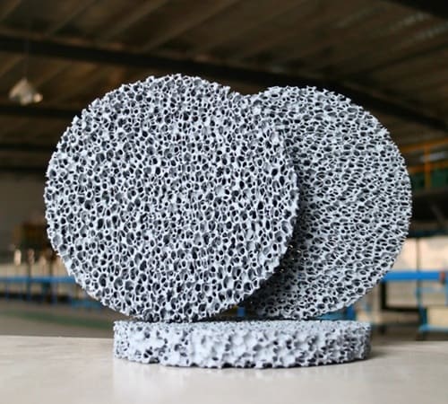
Silicon Carbide Sputtering Target Features
- High Purity: Ensures high-quality thin-film deposition with minimal impurities.
- Excellent High-Temperature Resistance: Remains stable in high-temperature deposition environments, suitable for demanding processes.
- High Hardness and Wear Resistance: Produces coatings with superior mechanical strength and durability.
- Good Chemical Stability: Corrosion-resistant, ideal for thin-film preparation in various chemical environments.
- High Thermal Conductivity: Efficient heat dissipation, suitable for coatings in high-power devices.
- Wide Bandgap Properties: Supports the production of high-performance semiconductor and optical films.
Silicon Carbide Sputtering Target Applications
- Semiconductor Manufacturing: Depositing SiC thin films for high-performance power and RF devices.
- Optical Coatings: Producing wear-resistant, high-temperature optical films, such as infrared windows and lenses.
- Photovoltaic Industry: Used for anti-reflective coatings and protective layers in solar cells to enhance efficiency and durability.
- Hard Coatings: Applied to tools and mechanical parts to improve wear resistance and lifespan.
- Microelectronics: Used in high-precision circuits and sensors for insulating or conductive layers.



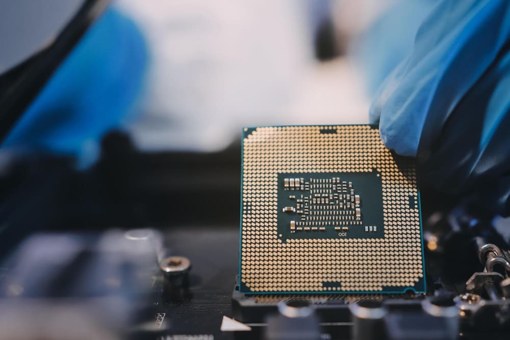
Silicon Carbide Sputtering Target Packaging
Silicon carbide foam filter products are typically packaged in vacuum-sealed bags to prevent moisture or contamination and wrapped with foam to cushion vibrations and impacts during transport, ensuring the quality of products in their original condition.

Download
- SAFETY DATA SHEET (SDS) -Silicon Nitride Custom Parts
FAQ
What are the main application fields of silicon carbide sputtering targets?
What core advantages does it have compared with traditional metal sputtering targets?
What are the common processes for preparing silicon carbide sputtering targets?
The mainstream ones are hot pressing sintering and spark plasma sintering (SPS), which can achieve high density and uniform microstructure of the target.
Which key performance indicator of the target should be focused on during use?
Why is the cost of silicon carbide sputtering targets usually high?
Get A Quote
Request a personalized quote tailored to your specific requirements.