
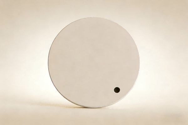
Aluminum Nitride Electrostatic Chuck
- Custom and standard options available.
- Fast lead times guaranteed.
- High performance at a competitive price.
Aluminum Nitride Electrostatic Chuck features excellent thermal conductivity, high insulation strength, and superior RF performance. It is designed for advanced semiconductor manufacturing, wafer processing, and high-precision electronic equipment production. NexusX Advanced Materials, as a premier manufacturer and supplier of high-quality aluminum nitride products, focuses on producing high-precision aluminum nitride electrostatic chucks for diverse application fields.
Or email us at [email protected]
Aluminum Nitride Electrostatic Chuck Data Sheet
| Density: | 3.3 g/cm3 |
| Appearance: | Greyish White, Beige |
| Thermal Conductivity: | 170-230 W/m·K |
Aluminum Nitride Electrostatic Chuck Description
As a critical component in advanced semiconductor manufacturing, the Aluminum Nitride Electrostatic Chuck (AlN ESC) uses high-purity aluminum nitride as its base material, which endows it with outstanding thermal conductivity for efficient heat dissipation, strong electrical insulation to avoid current leakage, and exceptional resistance to high temperatures (withstanding over 800°C in some cases); it relies on electrostatic force to firmly and evenly hold wafers, eliminating mechanical clamping damage while enabling ultra-precise temperature control (with a temperature stability of ±0.1°C), and is widely applied in key processes like wafer lithography, plasma etching, and thin-film deposition, significantly boosting chip production accuracy and yield.
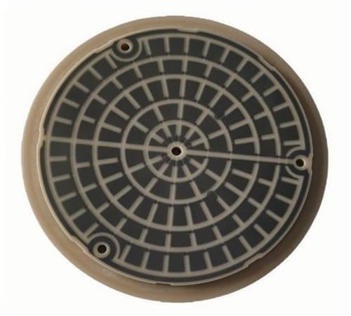
Aluminum Nitride Electrostatic Chuck Advantages
- High processing consistency
- Strong resistance to plasma erosion
- High mechanical strength
- Customizable
Aluminum Nitride Electrostatic Chuck Applications
- Semiconductor Lithography: It securely holds wafers during photoresist coating, exposure, and development, maintaining ultra-stable temperature (±0.1°C accuracy) to prevent wafer warping and ensure pattern transfer precision.
- Plasma Etching: Resists harsh plasma environments and high temperatures (up to 800°C), while its high thermal conductivity dissipates heat from etching reactions in real time, avoiding local overheating that damages wafer circuits.
- Thin-Film Deposition: Enables uniform electrostatic adsorption of wafers, ensuring consistent contact between the wafer surface and deposition sources (e.g., CVD/PVD systems), which improves the uniformity and quality of thin films (e.g., metal or dielectric films).
- Wafer Inspection & Testing: Provides damage-free clamping for post-process wafers, allowing high-precision optical or electrical testing without scratching or deforming the wafer surface.


Aluminum Nitride Ceramic Packaging
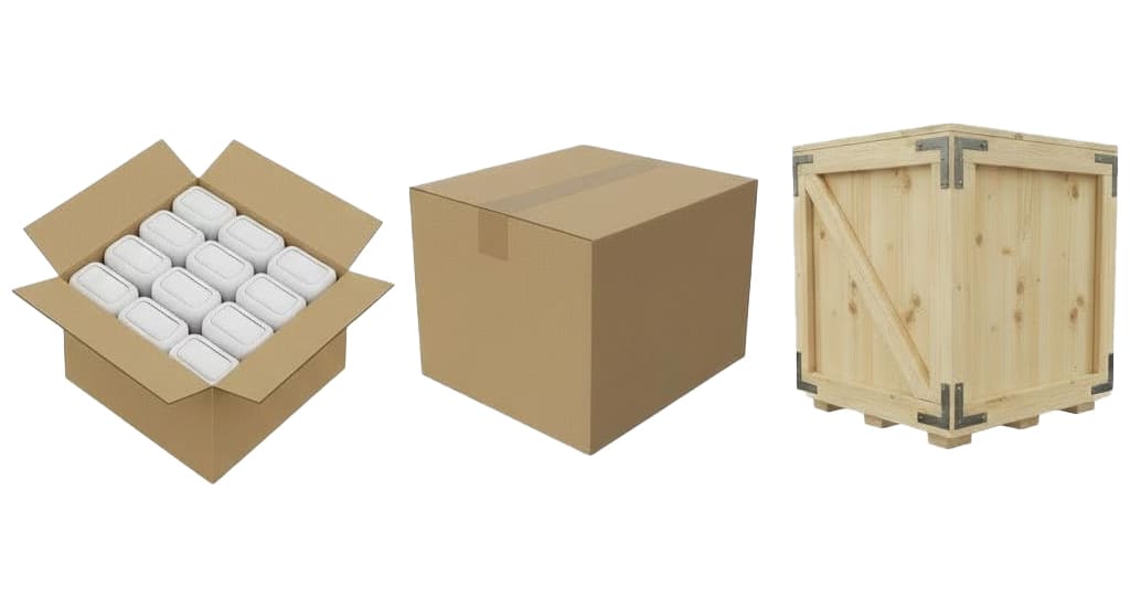
Aluminum Nitride Ceramic products are typically packaged in vacuum-sealed bags to prevent moisture or contamination and wrapped with foam to cushion vibrations and impacts during transport, ensuring the quality of products in their original condition.
Download
- SAFETY DATA SHEET (SDS) -Aluminum Nitride Electrostatic Chuck
FAQ
What makes aluminum nitride (AlN) the preferred base material for electrostatic chucks?
AlN offers a unique combination of high thermal conductivity (for efficient heat dissipation), strong electrical insulation (to prevent current leakage), and excellent high-temperature resistance (withstanding over 800°C), which matches the strict demands of semiconductor wafer processing.
How does an Aluminum Nitride ESC secure wafers, and what advantage does this method have over mechanical clamping?
In semiconductor manufacturing, which specific processes rely heavily on Aluminum Nitride ESCs?
What level of temperature control can an Aluminum Nitride ESC achieve, and why is this precision important?
It typically achieves temperature stability of ±0.1°C. This precision prevents wafer warping, ensures uniform photoresist coating/etching, and avoids thermal damage to delicate wafer circuits—all essential for producing high-performance, defect-free chips.
Can Aluminum Nitride ESCs be used with different wafer sizes, and do they require special maintenance?
Yes, they are designed to adapt to common wafer sizes (e.g., 8-inch, 12-inch) via adjustable electrostatic force. Maintenance mainly involves regular cleaning of the chuck surface to remove residue (e.g., etching byproducts) and checking insulation performance to avoid functional failures.
Get A Quote
Request a personalized quote tailored to your specific requirements.