
Aluminum Nitride Sputtering Target
- Custom and standard options available.
- Fast lead times guaranteed.
- High performance at a competitive price.
Or email us at [email protected]
Aluminum Nitride Sputtering Target Data Sheet
| Purity: | 99.5%-99.9% |
| Density: | 3.26 g/cm3 |
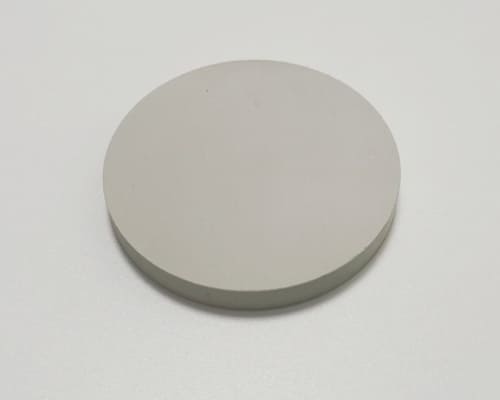
| Appearance: | Bluish White, Crystalline Solid |
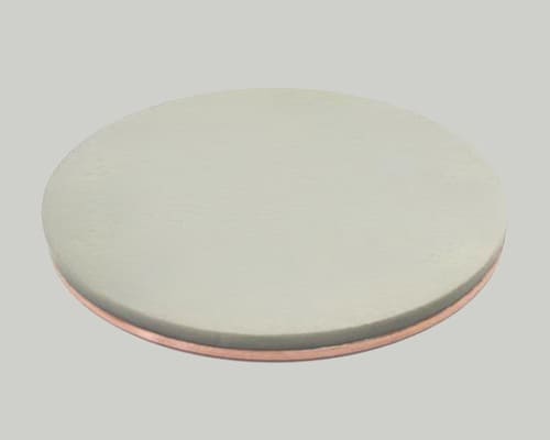
| Shape: | Rectangular, Disc, or Tube |
| Bonding Service: | Unbonding, or Bonding |
| Melting Point: | >2200℃ |
| Z Ratio: | 1.00 |
| Sputter: | RF-R |
| Max Power Density: | 20 W/in² |
Aluminum Nitride Sputtering Target Description
The Aluminum Nitride (AlN) Sputtering Target is a high-purity ceramic component critical for physical vapor deposition (PVD) processes, typically crafted with ≥99.5% pure AlN to minimize impurities. It is designed for compatibility with magnetron sputtering systems, it enables the deposition of dense, uniform AlN thin films onto substrates like silicon wafers or metal foils. These films inherit AlN’s key properties—exceptional thermal conductivity (≈170 W/m·K), strong electrical insulation, and resistance to high temperatures/corrosion—making the target indispensable for manufacturing semiconductor heat spreaders, LED epitaxial layers, and high-frequency device insulators, while its structural uniformity ensures consistent sputtering rates, directly supporting stable, high-yield thin-film production.
Aluminum Nitride Sputtering Target Specifications
| Circular Sputtering Targets | Diameter | 1.0″ 2.0″ 3.0″ 4.0″ 5.0″ 6.0″ up to 21″ |
| Rectangular Sputtering Targets | Width x Length | 5” x 12″ 5” x 15″ 5” x 20″ 5” x 22″ 6” x 20″ |
| Thickness | 0.125″, 0.25″ | |
Aluminum Nitride Sputtering Target Features
- High purity and density
- Low particle
- Uniform film thickness distribution
- High efficiency in the use
Aluminum Nitride Sputtering Target Applications
- Semiconductor Device Thermal Management: Used to deposit AlN thin films as heat spreaders or thermal interface layers on semiconductor chips (e.g., CPUs, power ICs). The films’ high thermal conductivity (≈170 W/m·K) efficiently transfers heat from high-power components, preventing overheating and ensuring stable device operation.
- LED and Optoelectronic Manufacturing: Enables deposition of AlN buffer layers in gallium nitride (GaN)-based LED epitaxy. The AlN film’s lattice matching with GaN reduces crystal defects, enhances light emission efficiency, and improves the long-term reliability of LEDs, especially high-brightness and ultraviolet (UV) LEDs.
- High-Frequency Electronic Components: Creates insulating AlN thin films for radio frequency (RF) devices (e.g., RF filters, microwave transistors) and 5G communication modules. The film’s excellent electrical insulation and low dielectric loss minimize signal interference, supporting high-frequency signal transmission with low attenuation.
- Power Electronic Packaging: Deposits AlN films as insulating and heat-dissipating layers in power device packaging (e.g., IGBTs, SiC modules). The films isolate high-voltage components while conducting heat away, balancing electrical insulation and thermal management to boost the durability of power electronics.
- Sensor and MEMS Fabrication: Used in manufacturing microelectromechanical systems (MEMS) and high-temperature sensors. AlN thin films’ high-temperature resistance (up to 800°C+) and chemical inertness allow sensors to operate stably in harsh environments (e.g., automotive engine compartments, industrial furnaces).





Aluminum Nitride Ceramic Packaging
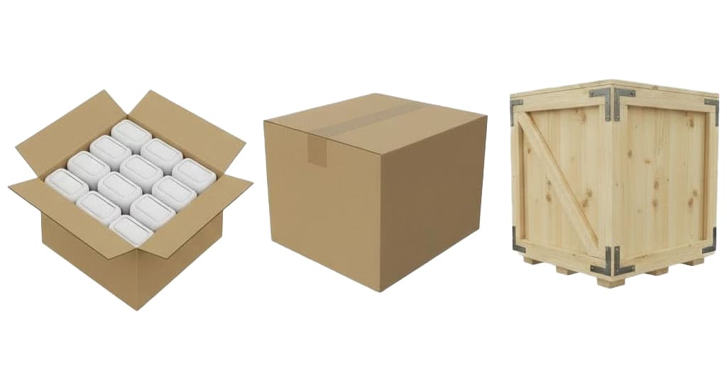
Aluminum Nitride Ceramic products are typically packaged in vacuum-sealed bags to prevent moisture or contamination and wrapped with foam to cushion vibrations and impacts during transport, ensuring the quality of products in their original condition.
Download
- SAFETY DATA SHEET (SDS) -Aluminum Nitride Sputtering Target
FAQ
What’s the typical purity of Aluminum Nitride Sputtering Targets, and why does it matter?
Usually ≥99.5% (high-end ≥99.9%). Impurities would contaminate thin films, ruining their thermal/insulation performance for devices like semiconductors.
Which sputtering tech pairs most with Aluminum Nitride Sputtering Targets, and what’s the benefit?
Why use Aluminum Nitride Sputtering Targets for GaN LED buffer layers?
How do Aluminum Nitride films improve RF devices?
AlN films have great insulation and low dielectric loss, minimizing signal interference/attenuation for stable 5G high-frequency transmission.
What target feature ensures consistent deposition?
Uniform microstructure (no cracks, even grains). It guarantees steady sputtering rates, avoiding uneven films that hurt product yield.
Get A Quote
Request a personalized quote tailored to your specific requirements.